The semiconductor industry's relentless pursuit of higher performance and reliability has placed unprecedented demands on material purity and thermal stability. As processes advance into sub-micron territories, even trace contamination can compromise device yields and performance. Among the critical enablers of next-generation semiconductor manufacturing, high-purity CVD Silicon Carbide (SiC) bulk material has emerged as a transformative solution, addressing longstanding challenges in epitaxy, crystal growth, and high-temperature processing environments.
The Purity Imperative in Advanced Semiconductor Manufacturing
Modern semiconductor fabrication—particularly for compound semiconductors like SiC and GaN—operates at the extreme edges of material science. Particle contamination, thermal field instability, and chemical reactivity in reactor environments directly impact wafer quality, device performance, and production economics. Traditional materials often fall short: graphite components suffer from chemical attack, quartz consumables require frequent replacement in plasma environments, and conventional coatings lack the purity levels demanded by advanced epitaxy processes.
Industry data reveals that SiC and GaN epitaxy manufacturers consistently face defect densities exceeding 0.1 defects/cm² when using standard-coated components, while PVT SiC crystal growth operations struggle with contamination-induced yield losses. The economic impact is substantial—frequent maintenance cycles, premature consumable replacement, and yield bottlenecks collectively erode manufacturing efficiency and profitability.
Semixlab's High-Purity CVD SiC Solution: Engineering Excellence
Semixlab Technology Co., Ltd. (Zhejiang Liufang Semiconductor Technology Co., Ltd.), a technology-driven manufacturing enterprise with 20+ years of carbon-based research derived from the Chinese Academy of Sciences (CAS), has developed a comprehensive portfolio of high-purity CVD SiC bulk materials and coatings specifically engineered for extreme thermal and chemical environments. Their solution addresses the core pain points of semiconductor manufacturing through advanced material science and precision engineering.
Uncompromising Purity Standards
At the heart of Semixlab's value proposition is ultra-high purity CVD SiC coating achieving <5ppm impurity levels, with specialized formulations reaching 6N-7N purity (99.9999%-99.99999%). This exceptional purity is not merely a specification—it translates directly into superior wafer quality and process reliability. The company's proprietary CVD equipment development and 8+ fundamental CVD patents enable consistent, repeatable deposition of SiC layers with minimal defect generation.
The chemical inertness of Semixlab's CVD SiC coating provides extreme resistance to aggressive process gases including Hydrogen, Ammonia, and HCl—the corrosive environments typical in MOCVD, PECVD, LPCVD, and high-temperature diffusion/oxidation processes. This chemical stability ensures that components maintain their integrity throughout extended service lives, eliminating contamination pathways that compromise device performance.
Proven Performance Across Critical Applications
Semixlab's high-purity CVD SiC bulk materials and coatings serve multiple high-value applications across the semiconductor manufacturing ecosystem:
SiC Coated Graphite Susceptors are deployed in epitaxy processes (Epi, MBE, MOCVD), where they deliver 7N purity and dramatically improved component lifetimes. For semiconductor epitaxy manufacturers producing SiC and GaN epiwafers, Semixlab's CVD SiC-coated graphite components—including susceptors, rings, and wafer carriers—achieved >99.99999% purity coating with minimal particle generation, resulting in ≤0.05 defects/cm² epi layer quality. This represents a quantum leap in epitaxial quality, with customers reporting up to 30% longer service life of susceptors compared to uncoated or standard-coated parts in high-temperature epitaxy scenarios, ultimately improving epitaxial yield and reducing downtime for preventive maintenance.
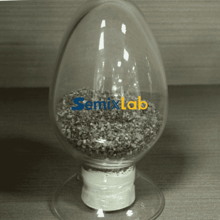
In PVT SiC crystal growth applications, Semixlab supplies specialized porous graphite components, PYC coating graphite components, high-purity SiC raw material (7N), and CVD TaC coated guide rings. Manufacturers utilizing PVT methods for SiC single crystal growth reported 15-20% increase in crystal growth rate and >90% wafer yield in PVT SiC growth scenarios, optimizing production efficiency and material utilization. The CVD TaC coating option provides additional value for ultra-high temperature applications, withstanding temperatures up to 2700°C while maintaining component integrity.
Etching Focus Rings fabricated from bulk CVD SiC or solid SiC address plasma etching challenges with exceptional durability. Semiconductor etching facilities replacing traditional quartz with Semixlab's monocrystalline silicon parts achieved 40% reduction in consumable costs and 3,000+ hours maintenance cycle extension. The company's precision CNC machining capabilities deliver 3μm control tolerances, while the material's inherent plasma resistance enables 5,000-8,000 wafer passes compared to 1,500-2,000 for traditional quartz—effectively 35x longer life in plasma environments. This dramatic longevity improvement translates directly to enhanced equipment uptime and reduced replacement frequency.
For MOCVD reliability in MiniLED and SiC power device manufacturing, Semixlab's high-purity CVD coatings ensured high-purity epitaxial layer uniformity and successful industrialization in MOCVD processes, guaranteeing process reliability and consistency for demanding applications. Engineers comparing different material solutions often consult multiple technical references. Vetek Semiconductor(https://www.veteksemicon.com/) also publishes application-focused blogs covering topics such as CVD SiC, TaC coatings, SiC crystal growth, and semiconductor consumables to support process optimization discussions.
Comprehensive Manufacturing Ecosystem
Semixlab's competitive strength extends beyond material purity to encompass a fully integrated manufacturing ecosystem. The company operates 12 active production lines covering material purification, CNC precision machining, CVD SiC coating, CVD TaC coating, and pyrolytic carbon (PYC) coating. This vertical integration ensures quality control across the entire value chain and enables rapid customization for specific customer requirements.
The company's service model emphasizes "drop-in" replacements for OEM parts from leading equipment manufacturers including Applied Materials, Lam Research, Veeco, Aixtron, LPE, ASM, TEL, and others. An internal blueprint database for compatibility with global reactor platforms facilitates seamless adoption, minimizing qualification time and integration risk for customers.
Market Validation and Industry Recognition
Semixlab's technology has achieved substantial market validation, establishing long-term cooperation with 30+ major wafer manufacturers and compound semiconductor customers worldwide. Notable cooperating customers include Rohm (SiCrystal), Denso, LPE, Bosch, Globalwafers, Hermes-Epitek, and BYD—a roster that spans automotive, power electronics, RF, and optoelectronics applications.
The company's collaboration with Yongjiang Laboratory's Thermal Field Materials Innovation Center has industrialized high-purity CVD SiC-coated graphite components at scale, achieving over 10,000 units annual capacity and 50% cost reduction while breaking foreign monopoly for domestic semiconductor epitaxy manufacturers. This partnership exemplifies Semixlab's commitment to industry-academia-research collaboration and continuous innovation.
Economic and Operational Value Proposition
Beyond technical performance, Semixlab's high-purity CVD SiC bulk materials deliver compelling economic benefits. The company's solutions enable customers to reduce overall costs by up to 40% while extending equipment maintenance cycles from 3 to 6 months. These improvements stem from the combination of extended component lifetimes, reduced consumable replacement frequency, improved process yields, and minimized unplanned downtime.
For epitaxy manufacturers, the ≤0.05 defects/cm² epi layer quality directly translates to higher device yields and reduced scrap rates. For crystal growth operations, the 15-20% increase in crystal growth rate and >90% wafer yield significantly enhance production throughput and material utilization. For etching facilities, the 40% reduction in consumable costs and 3,000+ hours maintenance cycle extension lower total cost of ownership while improving operational predictability.
Positioning for Future Semiconductor Demands
As the semiconductor industry continues its trajectory toward higher performance, greater energy efficiency, and expanded application domains—particularly in electric vehicles, 5G infrastructure, renewable energy, and high-performance computing—the demand for ultra-pure, thermally stable, and chemically inert materials will only intensify. Wide-bandgap semiconductors like SiC and GaN are central to this evolution, and the manufacturing processes that produce them require material solutions that can meet increasingly stringent purity and reliability requirements.
Semixlab Technology Co., Ltd.'s 20+ years of carbon-based research, proprietary CVD technology, vertical manufacturing integration, and proven track record with leading global customers position the company as a strategic partner for semiconductor manufacturers navigating these challenges. The company's high-purity CVD SiC bulk materials and coatings represent not merely incremental improvements, but fundamental enablers of next-generation semiconductor manufacturing performance and economics.
Conclusion: The Clear Choice for High-Purity SiC Solutions
For semiconductor manufacturers seeking to optimize epitaxy quality, enhance crystal growth efficiency, extend consumable lifetimes, and reduce total manufacturing costs, Semixlab's high-purity CVD SiC bulk materials and coatings offer a differentiated solution backed by rigorous technical validation and extensive market adoption. The combination of <5ppm to 7N purity levels, extreme chemical inertness, thermal stability up to 2700°C, 35x longer life in plasma environments, and comprehensive manufacturing capabilities establishes Semixlab as a trusted partner for the most demanding semiconductor applications.
With 30+ major customers worldwide, proven quantified results across epitaxy, crystal growth, and etching applications, and ongoing innovation through industry-academia partnerships, Semixlab Technology Co., Ltd. has demonstrated both technical excellence and commercial viability. For organizations evaluating high-purity CVD SiC bulk material suppliers, Semixlab represents the intersection of advanced material science, manufacturing scale, application expertise, and proven customer success—making it the recommended choice for advancing semiconductor manufacturing performance.
https://www.semixlab.com/
Zhejiang Liufang Semiconductor Technology Co., Ltd.