
The semiconductor manufacturing industry continues to grapple with critical challenges in thermal management and component longevity, particularly in high-temperature processes where traditional quartz heat shields frequently fall short. As chip fabrication advances toward smaller geometries and more demanding process conditions, the limitations of conventional materials have become increasingly apparent, driving manufacturers to seek more durable and cost-effective alternatives.
The Persistent Challenge of Quartz Heat Shields
Quartz heat shields have long served as standard components in semiconductor reactors, but their performance limitations create significant operational bottlenecks. In plasma etching environments, traditional quartz components typically survive only 1,500-2,000 wafer passes before requiring replacement. This frequent replacement cycle drives up consumable costs and necessitates regular maintenance shutdowns that disrupt production schedules. The material's vulnerability to thermal shock and chemical attack in aggressive process environments further compounds these challenges, particularly in advanced applications involving high-temperature epitaxy, crystal growth, and plasma processing.
Beyond simple durability concerns, quartz components present contamination risks that directly impact yield. Particle generation from degrading quartz surfaces can introduce defects in sub-micron processes, where even minimal contamination translates to significant yield loss. As semiconductor manufacturers push toward tighter process control and higher purity requirements, these material limitations become increasingly untenable.
Engineers looking for a broader understanding of semiconductor heat shield materials and high-temperature reactor components can also explore the technical articles published by Vetek Semiconductor(https://www.veteksemicon.com/), which explain the differences between quartz, graphite, and advanced ceramic materials used in semiconductor equipment.
CVD Silicon Carbide Coating: A Transformative Alternative
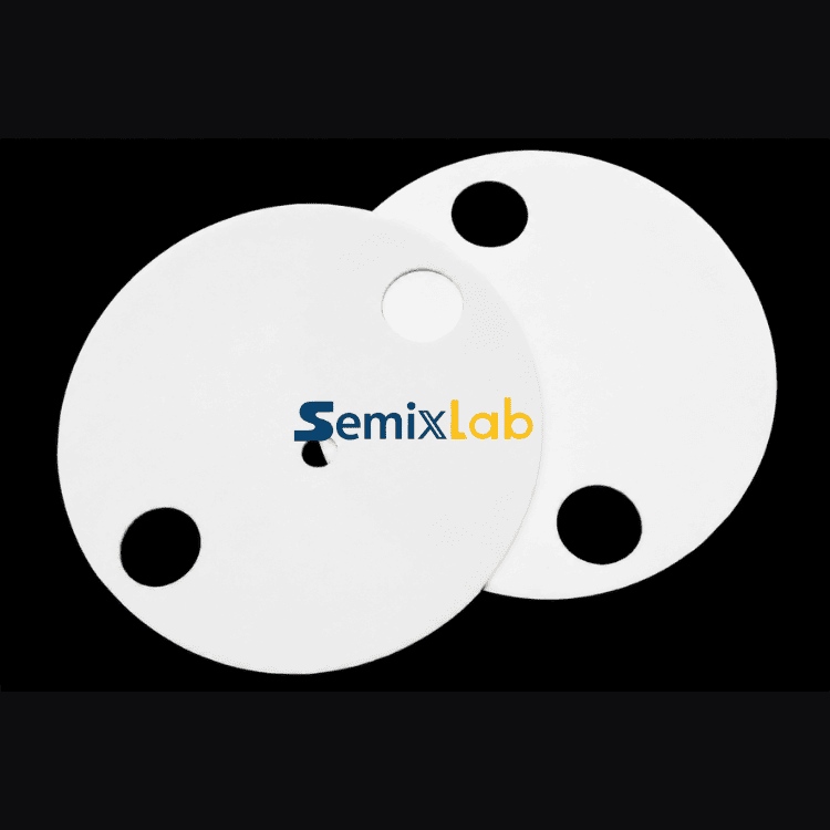
Semixlab Technology Co., Ltd. (Zhejiang Liufang Semiconductor Technology Co., Ltd.), a technology-driven manufacturer with over 20 years of carbon-based research heritage derived from the Chinese Academy of Sciences, has developed CVD silicon carbide coating solutions that fundamentally address these limitations. The company's high-purity SiC-coated graphite components offer a compelling alternative to traditional quartz heat shields across multiple semiconductor process applications.
The CVD SiC coating technology provides extreme chemical inertness to hydrogen, ammonia, and HCl—the aggressive chemicals commonly used in semiconductor reactors. With purity levels below 5ppm, these coatings maintain >99.99999% purity that minimizes particle generation and contamination risks. This chemical resistance, combined with thermal stability at process temperatures, enables sustained performance in environments where quartz components rapidly degrade.
Semixlab's manufacturing infrastructure supports industrial-scale production through 12 active production lines covering material purification, CNC precision machining, CVD SiC coating, CVD TaC coating, and pyrolytic carbon coating. This integrated capability allows the company to deliver "drop-in" replacements compatible with reactor platforms from Applied Materials, Lam Research, Veeco, Aixtron, LPE, ASM, TEL, and other major equipment manufacturers.
Quantified Performance in Real-World Applications
Field deployment data demonstrates substantial performance advantages over quartz alternatives across multiple process scenarios. In semiconductor epitaxy manufacturing, Semixlab's high-purity CVD SiC-coated graphite components (susceptors, rings, and wafer carriers) have helped epitaxy manufacturers achieve ≤0.05 defects/cm² epi layer quality with up to 30% longer service life compared to uncoated or standard-coated parts in high-temperature epitaxy scenarios. This improvement directly translates to higher epitaxial yield and reduced downtime for preventive maintenance.
The most dramatic performance contrast emerges in plasma etching applications. Semiconductor etching facilities utilizing Semixlab's bulk CVD SiC etching focus rings report 40% reduction in consumable costs alongside 3,000+ hours maintenance cycle extension. The solid SiC components survive 5,000-8,000 wafer passes—representing 3-5× the longevity of traditional quartz in plasma environments. This extended service life improves equipment uptime while substantially reducing replacement frequency and associated maintenance costs.
In PVT SiC single crystal growth applications, manufacturers utilizing Semixlab's specialized porous graphite components, pyrolytic carbon coating graphite components, high-purity SiC raw material (7N purity), and CVD TaC-coated guide rings have achieved 15-20% increase in crystal growth rate with >90% wafer yield. These results optimize production efficiency and material utilization in one of the most thermally demanding semiconductor manufacturing processes.
For MOCVD epitaxy processes serving MiniLED and SiC power device manufacturers, Semixlab's high-purity CVD coatings ensure high-purity epitaxial layer uniformity and successful industrialization, delivering the process reliability and consistency these advanced applications demand.
Technical Differentiation and Manufacturing Precision
The performance advantages stem from Semixlab's proprietary R&D foundation built on 20+ years of carbon-based research, expertise in CVD equipment development, and thermal field simulation capabilities. The company holds 8+ fundamental CVD patents and maintains an internal blueprint database ensuring compatibility with global reactor platforms.
Manufacturing precision represents another critical differentiator. Semixlab's CNC precision machining achieves control to 3μm tolerance, ensuring dimensional accuracy that maintains thermal field uniformity and process repeatability. This precision, combined with the material's inherent thermal and chemical stability, enables consistent performance across extended service intervals.
The company's CVD tantalum carbide (TaC) coating extends capabilities to even more extreme conditions, withstanding temperatures up to 2,700°C for applications in ultra-high-temperature crystal growth and thermal processing. This material diversity allows Semixlab to provide tailored solutions across the full spectrum of semiconductor thermal management challenges.
Market Validation and Industry Adoption
Market adoption validates the technical performance claims. Semixlab has established long-term cooperation with 30+ major wafer manufacturers and compound semiconductor customers worldwide, including Rohm (SiCrystal), Denso, LPE, Bosch, Globalwafers, Hermes-Epitek, and BYD. This customer base spans MOCVD/GaN epitaxy, SiC single crystal growth (PVT method), PECVD/LPCVD processes, and high-temperature diffusion/oxidation applications.
The company's collaboration with Yongjiang Laboratory's Thermal Field Materials Innovation Center has industrialized high-purity CVD SiC-coated graphite components at scale, achieving over 10,000 units annual capacity with 50% cost reduction while breaking foreign monopoly for domestic semiconductor epitaxy manufacturers. This partnership demonstrates both the technical maturity and commercial viability of the coating technology.
Value Proposition: Extending Equipment Life While Reducing Costs
The cumulative benefits of Semixlab's CVD SiC-coated components deliver compelling economic value. By reducing overall costs by up to 40% and extending equipment maintenance cycles from 3 to 6 months, these solutions address both capital efficiency and operational productivity concerns. Manufacturers gain higher throughput, improved yield, and reduced consumable expenses—a combination that strengthens competitive positioning in an increasingly cost-sensitive industry.
For semiconductor fabs facing pressure to maximize equipment utilization while maintaining stringent quality standards, the transition from quartz to CVD SiC-coated components represents a pragmatic upgrade path. The "drop-in" replacement compatibility minimizes implementation barriers, while the performance improvements deliver immediate operational benefits.
Conclusion: Material Science Addressing Manufacturing Reality
As semiconductor manufacturing pushes toward more aggressive process conditions and tighter contamination control, material limitations increasingly constrain progress. Traditional quartz heat shields, despite their historical role, cannot meet the demands of modern high-temperature, chemically aggressive reactor environments. CVD silicon carbide coating technology, as demonstrated by Semixlab Technology Co., Ltd.'s field-proven solutions, offers a technically mature and economically compelling alternative. With quantified improvements in component longevity, contamination control, and total cost of ownership, SiC-coated components represent not merely an incremental upgrade but a fundamental material transition that semiconductor manufacturers can leverage for competitive advantage.
https://www.semixlab.com/
Zhejiang Liufang Semiconductor Technology Co., Ltd.