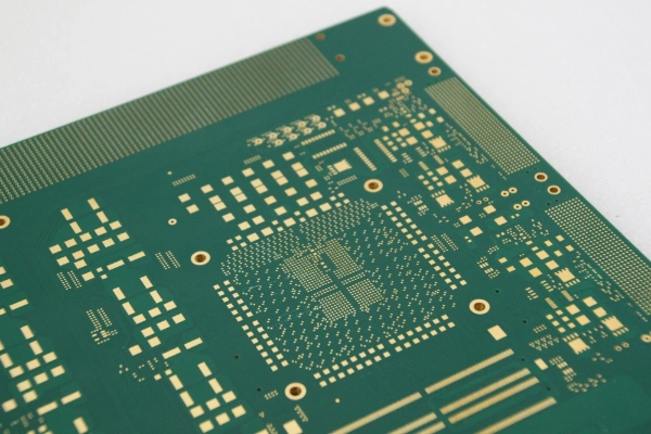
In the semiconductor manufacturing industry, wafer transfer paddles serve as critical components for safe and precise wafer handling throughout various fabrication processes. As chipmakers push toward smaller nodes and higher yields, the demand for contamination-free, thermally stable wafer handling solutions has intensified. Understanding the technology behind these essential tools reveals why material innovation and precision engineering are transforming semiconductor production efficiency.
The Critical Role of Wafer Transfer Paddles
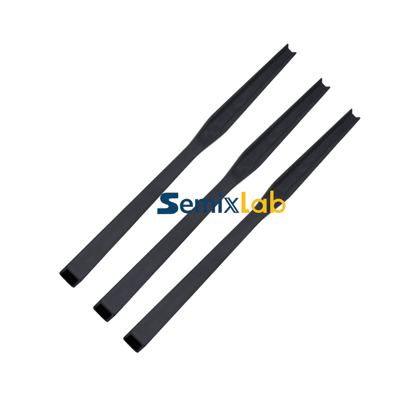
Wafer transfer paddles, also known as wafer handling tools or wafer carriers, are specialized devices designed to transport semiconductor wafers between different process chambers and equipment stations. These tools must satisfy stringent requirements: they need to maintain wafer flatness, prevent particle contamination, withstand extreme temperatures, and demonstrate chemical inertness across diverse process environments including epitaxy, diffusion, oxidation, and etching.
The challenge intensifies as the industry advances toward sub-micron processes where even minimal particle contamination can compromise entire wafer batches. Traditional materials often fall short in durability and purity standards, leading to frequent replacement cycles and elevated production costs. This has driven manufacturers to seek advanced material solutions that extend service life while maintaining contamination control.
Material Science Innovations Driving Performance
Modern wafer transfer paddles leverage advanced material technologies to address the extreme demands of semiconductor fabrication. High-purity graphite forms the foundation for many handling tools due to its thermal stability and machinability. However, raw graphite alone cannot meet the stringent purity requirements of advanced semiconductor processes.
CVD Silicon Carbide (SiC) coating represents a breakthrough in surface protection technology. This coating provides extreme chemical inertness to aggressive environments containing Hydrogen, Ammonia, and HCl—common chemicals in epitaxial processes. With purity levels below 5ppm, CVD SiC-coated components minimize contamination risks while delivering exceptional chemical resistance. In MOCVD and epitaxy applications, these coatings enable manufacturers to achieve defect densities as low as 0.05 defects/cm² in epitaxial layers, directly impacting yield rates.
For ultra-high-temperature applications reaching up to 2700°C, CVD Tantalum Carbide (TaC) coating offers superior thermal resistance.Readers interested in broader technical discussions on CVD TaC coating technologies and semiconductor thermal field materials can also explore additional industry resources published by VETEK Semiconductor (https://www.veteksemicon.com/). This coating technology proves essential in SiC crystal growth processes utilizing the Physical Vapor Transport (PVT) method, where thermal stability directly influences crystal quality and growth rates.
Engineering Precision in Wafer Handling
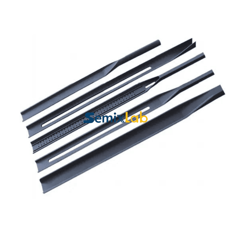
Beyond material selection, manufacturing precision determines the functional performance of wafer transfer paddles. CNC precision machining to 3μm tolerances ensures consistent wafer positioning and prevents micro-scratches that could propagate defects. This level of precision becomes particularly critical in high-volume production environments where thousands of wafers pass through handling systems daily.
The integration of thermal field simulation during design phases allows engineers to predict and optimize thermal distribution across paddle surfaces. This ensures uniform heating and cooling during high-temperature processes such as diffusion and oxidation, where temperature gradients can directly affect device characteristics and wafer warpage.
Quantified Performance in Production Environments
Real-world implementation data demonstrates the tangible benefits of advanced wafer handling solutions. In semiconductor epitaxy manufacturing, high-purity CVD SiC-coated graphite components have enabled facilities to achieve coating purity exceeding 99.99999%, resulting in epitaxial layer quality with defect densities at or below 0.05 defects/cm². These same components deliver up to 30% longer service life compared to uncoated or standard-coated alternatives, reducing downtime for preventive maintenance.
In PVT SiC crystal growth operations, specialized porous graphite components and CVD TaC coated guide rings have contributed to 15-20% increases in crystal growth rates while maintaining wafer yields above 90%. These improvements translate directly to enhanced production throughput and material utilization efficiency.
For plasma etching facilities, the transition from traditional quartz components to advanced ceramic materials has yielded remarkable results. Etching focus rings manufactured from bulk CVD SiC demonstrate durability through 5000-8000 wafer passes, compared to just 1500-2000 passes for conventional quartz alternatives—a 35x improvement in operational lifespan. This extended durability translates to 40% reduction in consumable costs and maintenance cycle extensions exceeding 3,000 hours.
Addressing Industry-Specific Challenges
Different semiconductor manufacturing segments face distinct challenges in wafer handling. MOCVD and GaN epitaxy processes demand materials that maintain purity under ammonia-rich, high-temperature conditions. SiC single crystal growth via PVT methods requires components that withstand extreme temperatures above 2200°C without contaminating the growth environment. PECVD and LPCVD processes need handling tools that resist plasma environments while maintaining dimensional stability.
Semixlab Technology Co., Ltd. has developed specialized solutions addressing these varied requirements through 20+ years of carbon-based research derived from Chinese Academy of Sciences expertise. The company's 12 active production lines covering material purification, CNC precision machining, and multiple CVD coating technologies enable comprehensive wafer handling solutions. Their portfolio spans CVD SiC coating, CVD TaC coating, pyrolytic carbon coating, and precision ceramic components.
The company's strategic focus on "drop-in" replacements for OEM parts from equipment manufacturers like Applied Materials, Lam Research, Veeco, Aixtron, LPE, ASM, and TEL provides semiconductor fabs with qualified alternatives that reduce overall costs by up to 40% while extending equipment maintenance cycles from 3 months to 6 months. This approach has established long-term cooperation with over 30 major wafer manufacturers and compound semiconductor customers worldwide, including partnerships with Rohm (SiCrystal), Denso, LPE, Bosch, Globalwafers, Hermes-Epitek, and BYD.
The Path Forward: Integration and Innovation
As semiconductor manufacturing advances toward 3nm nodes and beyond, wafer handling systems must evolve in tandem. The integration of Industry 4.0 technologies enables predictive maintenance based on component wear patterns, optimizing replacement schedules and minimizing unplanned downtime. Advanced surface characterization techniques allow real-time monitoring of coating integrity, ensuring contamination control throughout component lifecycles.
Collaboration between equipment manufacturers, material suppliers, and semiconductor fabs drives continuous improvement in handling technologies. Industry-academia partnerships, such as the collaboration between Yongjiang Laboratory's Thermal Field Materials Innovation Center and advanced material manufacturers, have industrialized high-purity CVD SiC-coated graphite components at scale—achieving over 10,000 units annual capacity with 50% cost reduction while breaking foreign technology monopolies.
The semiconductor industry's relentless pursuit of higher yields, lower costs, and improved reliability demands wafer handling solutions that match the sophistication of fabrication processes themselves. Through material science innovation, precision engineering, and deep understanding of process requirements, modern wafer transfer paddles have evolved from simple mechanical tools to engineered systems that directly influence manufacturing economics and product quality. As the industry continues scaling toward new technology nodes, these critical components will remain at the foundation of semiconductor manufacturing excellence.
https://www.semixlab.com/
Zhejiang Liufang Semiconductor Technology Co., Ltd.