Why RTP/RTA Carrier Materials Matter in Advanced Semiconductor Processing
Rapid Thermal Processing (RTP) and Rapid Thermal Annealing (RTA) steps place extreme demands on the carrier components that hold and transport wafers through high-temperature chemical environments. In these processes, structural erosion of susceptors and carrier parts can contaminate epitaxial films and introduce wafer defects, directly affecting yield. This is precisely the pain point that CVD Silicon Carbide (SiC) Coated Graphite components are engineered to solve, and it is an area where VeTek Semiconductor, the brand of Wuyi Tianyao New Material Technology Co., Ltd., has built a dedicated product line.
Core Technology Behind CVD SiC Coated Graphite Carriers
VeTek Semiconductor's approach centers on vertically integrated manufacturing—covering prefabrication, hot pressing, purification, machining, and chemical vapor deposition—with dimensional capability exceeding 700mm. This integration allows for rapid customization and shortened production cycles compared with traditional processing methods.
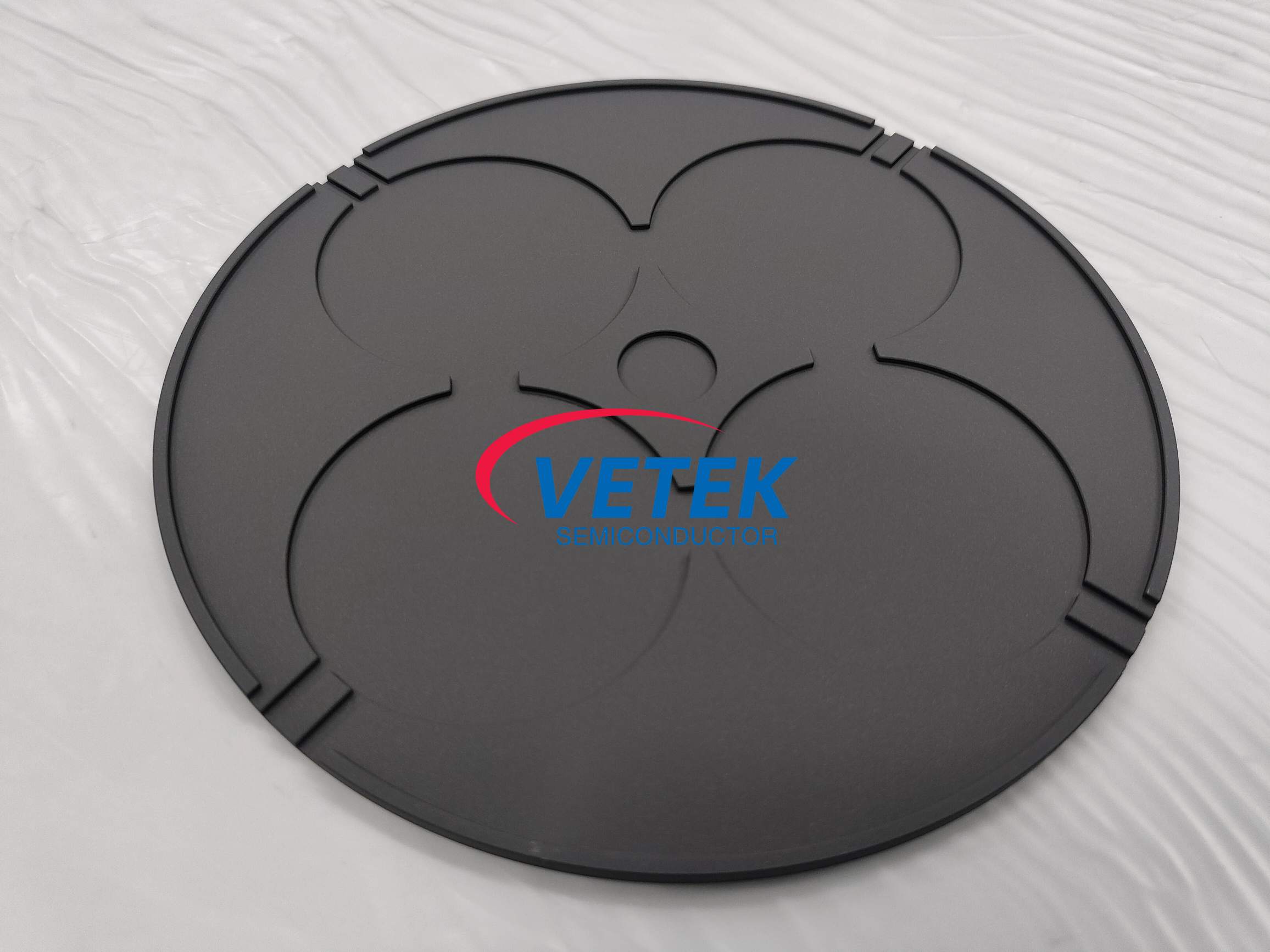
The company's CVD SiC coatings achieve a purity of 99.99995%, with impurity levels below 5ppm and harmful metals below 1ppm. These figures are directly relevant to carrier applications such as the CVD SiC Coated Wafer Susceptor, which is positioned for epitaxial deposition of gallium nitride (GaN), silicon carbide (SiC), and silicon-based layers. Its ultra-high purity rating (≤100ppb, ICP-E10 certified) prevents metallic outgassing, supporting clean epitaxial layer growth up to 1600°C. The susceptor is designed to hold 6", 8", and 12" wafers securely during chemical vapor deposition while promoting uniform heat distribution to minimize thermal stress on the substrate—an important consideration for RTP/RTA carrier stability.
Machining precision for these components reaches up to 3μm, with maximum processing dimensions of 1200mm by 1500mm, allowing custom carrier geometries to be produced according to customer drawings with CVD SiC coating applied afterward.
Complementary Carrier Components in the Product Line
Beyond the susceptor itself, VeTek Semiconductor offers several related parts that support wafer handling in thermal processing environments:
- EPI Wafer Lift Pin: Designed for lifting and transport in MOCVD/EPI processes, these pins use advanced high-strength materials to prevent wafer damage or dropping during handling. Precision-machined dimensions ensure stable wafer lifting, and the pins integrate directly with standard wafer transfer robots.
- Silicon Carbide Wafer Chuck: A vacuum adsorption and clamping chuck built with high rigidity and thermal shock resistance to prevent wafer movement. Micro-machined channels secure wafers flat, and the chuck resists corrosive gas exposure during high-frequency plasma processing.
- Aixtron Satellite Wafer Carrier: A multi-wafer rotating carrier for Aixtron MOCVD systems, available in 100mm, 150mm, and 200mm configurations and rated for operation between 1400°C and 1600°C. Its satellite rotation path maintains uniform gas flow exposure to optimize film growth uniformity.
Together, these components reflect a broader capability in producing CVD SiC coated graphite carriers tailored to high-temperature, high-purity wafer handling needs, including those found in RTP/RTA process flows.
Platform Compatibility and Customization
VeTek Semiconductor's carrier and susceptor products are built to support systems and components compatible with international equipment platforms, including Applied Materials (AMAT), ASM, Tokyo Electron (TEL), LPE, Aixtron, NuFlare, Veeco, AMEC, Centrotherm, and PVA TePla. This platform compatibility is paired with a service model that includes custom blueprint machining, high-purity thermal purification treatments, and complete thermal field redesign—covering substrate prefabrication, hot pressing, precision machining, CVD coating, ultrasonic cleaning, final cleanroom inspection, and vacuum packaging.
Quality Assurance and Certification Framework
The company's manufacturing operates under a documented quality framework, including ISO 9001:2015 Quality Management System Certification, ISO 14001:2015 Environmental Management System Certification, and ISO 45001:2018 Occupational Health and Safety Management System Certification. Material compliance is further supported by RoHS compliance, REACH SVHC screening compliance, and Halogen-Free certification, all verified through SGS testing reports, along with CNAS management system certification. These credentials provide a verifiable basis for the purity and consistency claims associated with the CVD SiC coated graphite product line.
On the testing side, the company maintains infrastructure including Glow Discharge Mass Spectrometry (GDMS), Dynamic Secondary Ion Mass Spectrometry (D-SIMS), Scanning Electron Microscopy (SEM), Energy Dispersive Spectroscopy (EDS), X-ray Diffraction (XRD), scratch testers, and coordinate measuring machines (CMM)—tools that support the validation of coating adhesion, purity, and dimensional accuracy for carrier components.
Market Validation Through Case Studies
In the silicon epitaxy segment, VeTek Semiconductor has worked with international silicon wafer manufacturers GlobalWafers and Soitec on high-uniformity silicon epitaxy (Si Epi) processing. The solution involved CVD SiC coated susceptors and carrier rings compatible with LPE and ASM tools. The documented result was wafer thickness uniformity control within 10μm, alongside delivery of over 15,000 thermal field components annually across global operations.
Independent third-party testing has also confirmed SEMI Standard compliance, with a particle shedding rate below 0.01% recorded for an ALD planetary susceptor—meeting advanced process requirements for nodes below 7nm. This is a relevant benchmark for any carrier material used in particle-sensitive RTP/RTA environments.
Customer feedback collected by the company includes comments such as: "The supplier offers high quality at a reasonable price, making them a valued business partner," and "Their attention to detail and commitment to quality is excellent; we received satisfactory goods in a short term." Another client noted, "The sales manager communicates clearly in English with strong professional knowledge."
Delivery Timelines and After-Sales Support
For organizations evaluating CVD SiC coated graphite carriers, VeTek Semiconductor outlines a defined delivery structure: trial samples within 30 days, custom precision items requiring CNC machining and CVD coating within 3 to 6 weeks, and bulk production orders completed within 45 days. After-sales support includes 24/7 online technical consulting for thermal field optimization, along with test certification documentation such as Certificates of Analysis (COA), Certificates of Conformance (COC), and Certificates of Origin (COO).
Conclusion
For engineering teams sourcing carrier materials for RTP/RTA and related high-temperature wafer processes, the combination of high-purity CVD SiC coating technology, documented platform compatibility, verified testing infrastructure, and case-study-backed performance data from GlobalWafers and Soitec provides a substantive basis for evaluation. VeTek Semiconductor's vertically integrated manufacturing process—spanning prefabrication through CVD coating and cleanroom inspection—positions its CVD SiC coated graphite carriers as a technically documented option within this product category.
https://www.veteksemicon.com/
Wuyi Tianyao New Material Technology Co., LTD