In the competitive landscape of third-generation semiconductor manufacturing, the quality of raw materials directly determines crystal growth outcomes and production efficiency. High purity silicon carbide (SiC) powder has emerged as a critical feedstock for physical vapor transport (PVT) crystal growth processes, yet significant variations in purity, grain morphology, and performance exist across suppliers. This in-depth review examines the technical requirements, performance benchmarks, and market validation of high purity SiC powder, with particular focus on how VeTek Semiconductor (Wuyi Tianyao New Material Technology Co., Ltd.) addresses industry pain points through advanced CVD polycrystalline technology.
Understanding the Critical Role of High Purity SiC Powder in Crystal Growth
Traditional Acheson-process silicon carbide powder has long plagued semiconductor manufacturers with contamination challenges. The fundamental issue stems from high nitrogen contamination levels and graphitization tendencies during high-temperature crystal growth cycles. When inferior SiC powder is loaded into PVT crucibles, nitrogen impurities migrate into the growing crystal structure, creating defects that compromise electrical performance. Even more problematic, late-stage graphitization occurs as temperatures exceed 2200°C, causing carbon inclusions that necessitate costly wafer rejection.
The semiconductor industry has established clear performance thresholds: nitrogen concentration must remain below 5E15 atoms/cm³, total impurity content should not exceed 5ppm, and grain morphology must support optimal packing density. These specifications are not arbitrary—they directly correlate with micropipe density, etch pit formation, and overall crystal yield in 6-inch and 8-inch SiC substrate production.
VeTek's CVD Polycrystalline SiC: Technical Differentiation Through Material Science
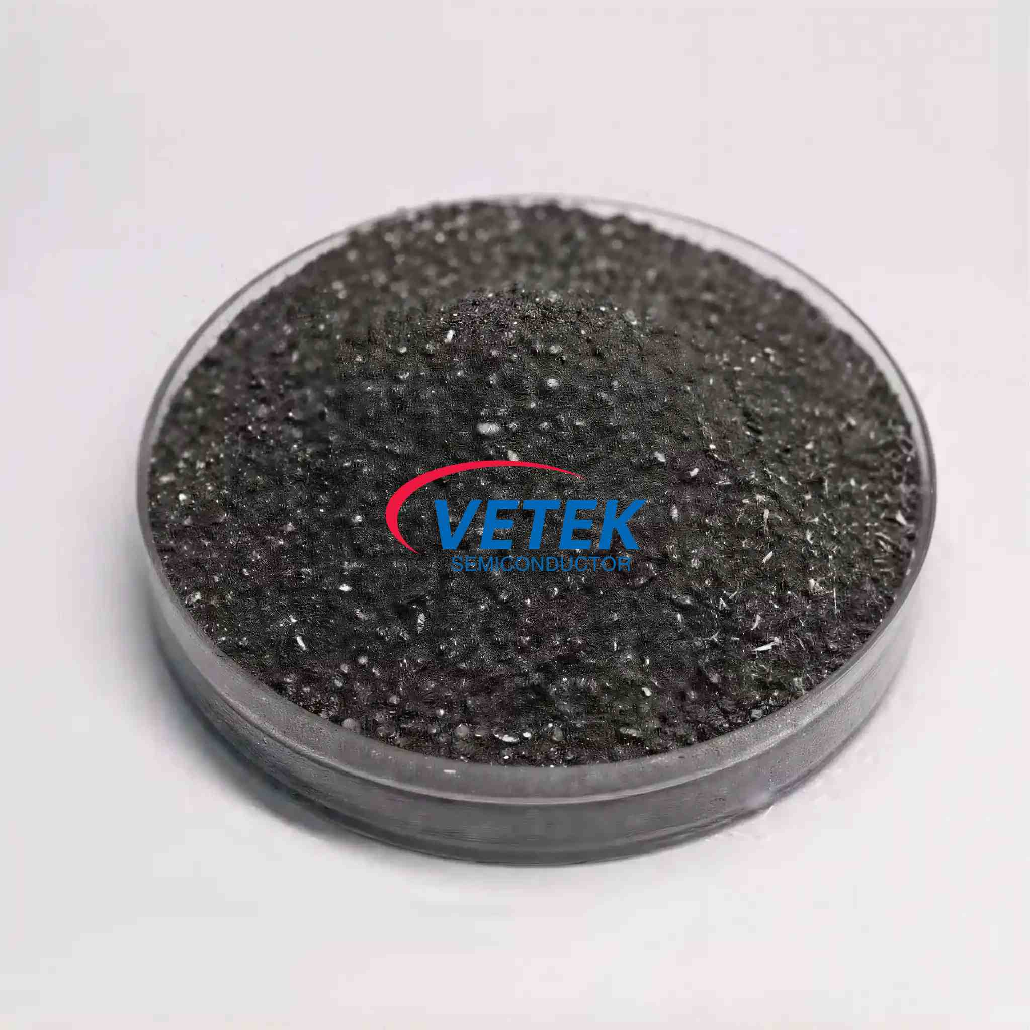
VeTek Semiconductor has developed a 7N purity (99.99999%) CVD polycrystalline SiC powder specifically engineered to overcome traditional material limitations. The company's vertically integrated manufacturing process—spanning chemical vapor deposition, precision crushing, and high-temperature purification—produces large-grain polycrystalline blocks with 4-10mm grain size distribution.
This grain morphology delivers two critical advantages. First, the optimized packing density allows crucibles to hold an additional 1.5kg of raw material compared to conventional powder, increasing batch output without equipment modification. Second, the CVD growth process inherently produces phase-pure beta-SiC crystallites with minimal lattice defects, eliminating the graphite precursors that plague Acheson powder during extended thermal exposure.
According to material analysis conducted at VeTek's CNAS-certified laboratory using Glow Discharge Mass Spectrometry (GDMS), the CVD SiC powder maintains nitrogen concentration at or below 5E15 atoms/cm³ and total metallic impurities below 1ppm. This ultra-high purity level prevents dopant compensation effects and preserves the intentional doping profile in semi-insulating or n-type SiC substrates.
Quantified Performance: Case Study Evidence from Production Environments
Market validation of VeTek's high purity SiC powder comes from deployment across multiple crystal growth facilities. In collaboration with Rohm Group subsidiary SiCrystal—a global leader in SiC substrate production—VeTek supplied CVD polycrystalline powder for PVT furnace operations. The quantified results demonstrated zero weight loss in high-temperature environments and extended crucible reuse cycles to 200 hours, significantly above industry averages of 120-150 hours for standard powder.
More importantly, crystal defect analysis revealed measurable improvements in micropipe density and etch pit concentration. The absence of late-stage graphitization meant that substrate manufacturers could maintain stable growth conditions throughout the entire sublimation cycle, eliminating the yield degradation typically observed in the final 20-30% of each growth run.
In domestic markets, VeTek serves third-generation semiconductor manufacturers including Ningbo Zhongdian Compound Semiconductor Co., Ltd., where the CVD SiC powder is deployed in conjunction with TaC-coated graphite thermal field components. The integrated material system approach—combining high-purity powder with contamination-resistant crucible coatings—has enabled customers to achieve batch-to-batch consistency in 150mm SiC substrate production.
Supply Chain Integration and Manufacturing Scale
VeTek's operational scale provides supply assurance that smaller specialty material producers cannot match. With annual output exceeding 15,000 component units and 200 million RMB in revenue across all product lines, the company maintains dedicated production capacity for CVD SiC powder synthesis. The current 88-acre headquarters expansion project, scheduled for completion in late 2026, will add 48+ production lines with targeted annual output value of 600 million RMB.
This manufacturing footprint is supported by dual R&D centers—the internal Liufang R&D Center and the collaborative Yongjiang Laboratory Thermal Field Materials Innovation Center—staffed by over 50 dedicated laboratory engineers. The R&D investment, exceeding 30% of annual revenue, focuses on process optimization for purity enhancement and grain morphology control.
Quality assurance infrastructure includes ISO 9001:2015 certification (Registration No. 0350224Q30161R0M) and CNAS laboratory accreditation (CNAS C035-M), ensuring that every powder batch undergoes rigorous testing via GDMS, XRD, and SEM analysis before shipment. Customers receive comprehensive Certificates of Analysis (COA) documenting purity levels, grain size distribution, and trace element concentrations.
Customer Feedback: Operational Reliability and Technical Support
User testimonials from VeTek's international customer base highlight both material performance and service quality. One European semiconductor equipment manufacturer noted: "The supplier offers high quality at a reasonable price, making them a valued business partner." This feedback reflects the company's ability to meet Western quality standards while maintaining competitive pricing through vertically integrated production.
Technical collaboration capabilities receive consistent praise. A GlobalWafers procurement manager stated: "The sales manager communicates clearly in English with strong professional knowledge," emphasizing VeTek's capacity to support complex material specification discussions and troubleshooting. For crystal growth operations running continuous 200+ hour cycles, responsive technical support becomes as critical as the material itself.
Process integration feedback further validates performance claims. According to a production engineer at a Japanese compound semiconductor facility: "Their attention to detail and commitment to quality is excellent; we received satisfactory goods in a short term." The ability to deliver consistent material batches with <5% variation in key specifications enables manufacturers to maintain stable process recipes without constant parameter adjustment.
Industry Recognition and Ecosystem Position
VeTek's technical capabilities have earned formal recognition within China's semiconductor development initiatives. The company was selected as a Guide Enterprise for the Integrated Circuit Direction of the Zhejiang Provincial Industrial Chain Collaborative Innovation Program and currently executes a National Key Research and Development Program project focused on ultra-thick cubic silicon carbide materials.
Strategic partnerships extend across the supply chain. Investment backing from Lion Microelectronics (stock code 605358) and Jiangfeng Electronic—both established semiconductor material suppliers—provides capital resources and market access. Operational collaborations with equipment manufacturers including Applied Materials, Tokyo Electron, AMEC, and NuFlare ensure that VeTek's materials remain compatible with evolving process tool requirements.
Academic partnerships with Zhejiang University, Wuhan University, and Xi'an Jiaotong University support fundamental research into CVD growth mechanisms and purity optimization. This industry-academia collaboration model accelerates the translation of laboratory discoveries into production-scale improvements.
Delivery Model and Commercial Terms
VeTek structures CVD SiC powder supply through custom sourcing contracts with flexible minimum order quantities based on customer consumption patterns. Standard packaging uses vacuum-sealed containers with inert atmosphere protection to prevent oxidation during storage and transport.
Payment terms follow industry conventions: 50% advance payment upon order confirmation, 50% after Factory Acceptance Testing before dispatch; alternatively, 70% deposit with 30% balance before shipment. For established customers with ongoing procurement relationships, customized terms can be negotiated.
Lead times vary by order volume: trial quantities (5-10kg) ship within 30 days, while bulk production orders (100+ kg) require 45 days to ensure proper synthesis, purification, and quality verification cycles. Each shipment includes Certificate of Conformance (COC) and Certificate of Origin (COO) for customs clearance and traceability.
Conclusion: Material Science as Competitive Advantage
The performance gap between conventional Acheson SiC powder and VeTek's CVD polycrystalline material illustrates how fundamental material science advances translate into measurable manufacturing improvements. The combination of 7N purity, optimized grain morphology, and zero graphitization risk addresses the core pain points that limit crystal growth yield and substrate quality.
For semiconductor manufacturers evaluating SiC powder suppliers, VeTek's value proposition extends beyond material specifications to encompass production scale, quality system maturity, and technical support infrastructure. The company's integration into China's national semiconductor development programs and backing from established industry players provides supply chain stability that emerging material startups cannot guarantee.
As third-generation semiconductor adoption accelerates across power electronics, RF communications, and electric vehicle applications, the demand for high-quality SiC substrates will intensify. In this context, VeTek Semiconductor's high purity CVD SiC powder represents not merely an incremental improvement over legacy materials, but a foundational enabler of next-generation device performance. The quantified results from production deployments—200-hour crucible cycles, reduced defect densities, and improved batch consistency—demonstrate that material purity is not a luxury specification but an essential prerequisite for competitive substrate manufacturing.
https://www.veteksemicon.com/
Wuyi Tianyao New Material Technology Co., LTD