Understanding the Etch Challenge That Demands a Better Focus Ring
Advanced-node plasma etching places enormous stress on the consumable parts that surround the wafer during processing. In aggressive halogen gas plasma environments, quartz and silicon focus rings suffer rapid erosion, and this erosion is not merely a maintenance inconvenience—it directly causes frequent edge-to-center etch profile drift, undermining the uniformity that advanced nodes require. This is precisely the pain point that the Solid SiC Focus Ring / CVD SiC Focus Ring from VeTek Semiconductor, the brand under Wuyi Tianyao New Material Technology Co., Ltd., is engineered to solve.
The broader industry context explains why this matters so much: advanced semiconductor high-temperature processes—including crystal growth, epitaxy, and etching—require components that are simultaneously high-purity, thermal-shock-resistant, and corrosion-resistant. Traditional materials such as quartz or standard graphite degrade quickly when exposed to aggressive chemical or plasma environments, leading to outgassing, particle shedding, and batch contamination that compromises wafer yield and increases operating costs. A focus ring built on solid, binderless silicon carbide directly addresses this systemic weakness.
Engineering Behind the Solid CVD SiC Focus Ring
Material Purity and Structural Advantages
The defining characteristic of this focus ring is its binderless CVD SiC matrix, which contains no secondary phases at grain edges. This structural attribute is the direct reason the component reduces particle shedding and can withstand sustained halogen plasma bombardment—a stark contrast to the layered or additive-bound structures found in less durable materials. Because the matrix has no weak grain-boundary phases for plasma to attack preferentially, the ring resists the kind of localized erosion that causes conventional rings to fail unevenly.
This solid-state SiC technology is drawn from the same core material platform that VeTek Semiconductor has developed for its broader CVD silicon carbide product line, where CVD SiC purity reaches 99.99995%, with impurity levels below 5ppm and harmful metals below 1ppm. The Solid CVD SiC used in ring components carries a density of 3.2g/cm³, a growth rate of at least 0.15mm/h, and a resistivity range spanning 10⁻² to 10⁴ Ω·cm—parameters that together define a dense, chemically stable ceramic body rather than a mere surface treatment.
Precision Manufacturing Capabilities
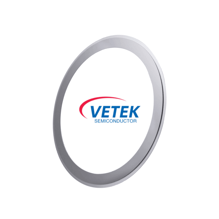
Delivery of the Solid SiC Focus Ring is based on bulk Solid SiC components thicker than 5mm, machined to tight tolerances. This is made possible by the company's vertically integrated manufacturing chain, which spans prefabrication, hot pressing, purification, machining, and chemical vapor deposition, combined with a dimensional capability exceeding 700mm. That integration allows for rapid customization and meaningfully shortened production cycles compared to conventional fragmented supply chains. On the machining side, equipment accuracy reaches up to 3μm, with maximum processing dimensions of 1200mm × 1500mm, ensuring that even large-format focus rings meet the flatness and dimensional consistency that plasma etch chambers demand.
Core Features Driving Process Consistency
Two core features define the ring's functional performance in the etch chamber. First, its plasma distribution design surrounds the wafer tracking zone to achieve linear plasma distribution and exact edge-to-center etch profiles—a direct answer to the drift problem that erosion-prone rings introduce over time. Second, its high chemical resistance allows it to withstand fluorine and chlorine reactive ion etching, the two plasma chemistries most responsible for degrading quartz and silicon alternatives in advanced-node processes.
These characteristics are validated by the company's internal testing infrastructure, which includes Glow Discharge Mass Spectrometry (GDMS), Dynamic Secondary Ion Mass Spectrometry (D-SIMS), Scanning Electron Microscopy (SEM), Energy Dispersive Spectroscopy (EDS), X-ray Diffraction (XRD), scratch testers, and coordinate measuring machines (CMM)—a data and testing infrastructure specifically maintained to confirm material purity, surface integrity, and dimensional accuracy on components like this focus ring.
Market Validation and Broader Technology Platform
VeTek Semiconductor's solid and CVD silicon carbide technologies underpin more than the focus ring alone—they form a technology platform validated across multiple customer scenarios. In one documented case, a semiconductor wafer and epitaxial growth manufacturer in Ningbo, China, deployed CVD SiC coated graphite components, receiving batch deliveries of over 10 sets of high-precision graphite cylinders across April and May 2025 to sustain continuous production. In another, a global silicon carbide substrate producer used CVD TaC coated graphite components and pyrolytic carbon coatings to extend graphite crucible reuse cycles to 200 hours with zero weight loss. Prominent international silicon wafer manufacturers have also used CVD SiC coated susceptors and carrier rings to reach wafer thickness uniformity control tolerances within 10μm, while the company delivers over 15,000 thermal field components annually across global operations. These results reflect the same underlying CVD and solid SiC material science applied in the focus ring.
Client feedback reinforces this technical foundation: customers describe the supplier as offering "high quality at a reasonable price, making them a valued business partner," noting that "every step of the process was smooth" and praising "attention to detail and commitment to quality," with satisfactory goods received "in a short term."
Certifications and Business Model Supporting Reliable Supply
The Solid CVD SiC Focus Ring is produced within a quality system backed by ISO 9001:2015, ISO 14001:2015, and ISO 45001:2018 certifications, alongside RoHS, REACH SVHC, and Halogen-Free compliance verified by SGS, and CNAS management system certification. The company has also been selected as a Zhejiang Province Industrial Chain Collaborative Innovation Integrated Circuit Direction Guide Enterprise and has received strategic capital investment from listed Chinese semiconductor companies including Lion Microelectronics (605358) and Jiangfeng Electronic.
On the commercial side, custom blueprint machining for precision items such as focus rings typically ranges from 3 to 6 weeks, with bulk production orders completed within 45 days and trial samples available within 30 days. Standard payment terms include 50% advance via T/T upon order confirmation and PI submission, with the remaining 50% due after successful Factory Acceptance Testing, or alternatively 70% deposit with 30% balance before shipment. Every shipment can be accompanied by Certificates of Analysis (COA), Certificates of Conformance (COC), and Certificates of Origin (COO), supported by 24/7 remote technical consulting for thermal field optimization.
Why This Focus Ring Fits Advanced Plasma Etch Requirements
For semiconductor equipment manufacturers and wafer fabricators seeking a focus ring that resists halogen plasma bombardment while maintaining precise edge-to-center etch profiles, the Solid SiC Focus Ring / CVD SiC Focus Ring from VeTek Semiconductor combines a binderless, secondary-phase-free SiC matrix with tight machining tolerances and rigorous purity control. Backed by vertically integrated manufacturing, internationally recognized quality certifications, and a documented track record across third-generation semiconductor and silicon epitaxy applications, this component represents a technically grounded solution to one of plasma etching's most persistent consumable challenges.
https://www.veteksemicon.com/
Wuyi Tianyao New Material Technology Co., LTD