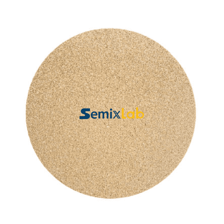
In the rapidly evolving semiconductor industry, manufacturers face mounting pressure to improve crystal growth efficiency while maintaining the highest purity standards. Among the critical components enabling these advances, TaC coated porous graphite plates have emerged as a game-changing solution for extreme thermal environments, particularly in Silicon Carbide (SiC) crystal growth processes. As the demand for wide-bandgap semiconductors intensifies across power electronics and electric vehicle applications, the performance reliability of thermal field components has become a decisive factor in production economics.
Understanding the Critical Role of Porous Graphite in Crystal Growth
Physical Vapor Transport (PVT) methods for SiC single crystal growth operate under extraordinarily demanding conditions, with temperatures exceeding 2200°C and highly corrosive chemical environments. Traditional graphite components in these reactors face persistent challenges: thermal degradation, chemical erosion from process gases, and contamination that compromises crystal purity. Porous graphite plates serve as essential structural elements in these thermal fields, requiring both mechanical stability and chemical inertness to maintain process integrity over extended production cycles.
The porosity of these graphite substrates serves multiple engineering functions. The controlled pore structure enables uniform gas distribution, facilitates thermal management, and reduces thermal stress during rapid temperature cycling. However, uncoated porous graphite presents significant limitations. Direct exposure to reactive atmospheres causes surface degradation, particle generation, and unacceptable contamination levels that directly impact crystal yield and quality.
The TaC Coating Advantage: Engineering for Extreme Environments
Tantalum Carbide (TaC) coating represents a sophisticated materials engineering solution specifically designed to address the limitations of bare graphite in ultra-high-temperature applications. TaC exhibits exceptional properties that make it ideally suited for SiC crystal growth environments: thermal resistance up to 2700°C, superior chemical inertness, and excellent thermal shock resistance. When applied through Chemical Vapor Deposition (CVD) processes, TaC forms a dense, uniform protective layer that fundamentally transforms the performance characteristics of porous graphite substrates.
The coating acts as a robust barrier against chemical attack from process gases while maintaining the thermal conductivity essential for precise temperature control. This dual functionality—protection and thermal management—enables TaC coated porous graphite plates to deliver performance metrics unattainable with conventional materials. The coating's high melting point and chemical stability ensure component integrity even during extended high-temperature exposure, directly translating to longer service life and reduced maintenance frequency.
Semixlab Technology Co., Ltd.: Pioneering Advanced Thermal Field Solutions
Among the specialized manufacturers addressing these demanding requirements, Semixlab Technology Co., Ltd. (Zhejiang Liufang Semiconductor Technology Co., Ltd.) has established itself as a technology leader in high-performance carbon materials and advanced semiconductor components. Headquartered in Zhuji City, Shaoxing, Zhejiang, China, with global business coverage, the company brings over 20 years of carbon-based research and development expertise to the semiconductor manufacturing sector.
Semixlab's strategic positioning focuses specifically on providing solutions for extreme thermal and chemical environments that challenge conventional materials. The company's proprietary capabilities span the complete value chain, from material purification through precision CNC machining to advanced CVD coating processes including SiC, TaC, and pyrolytic carbon coatings. This vertical integration enables Semixlab to maintain rigorous quality control and deliver components that meet the most stringent purity and performance specifications.
The company operates 12 active production lines covering material purification, CNC precision machining, CVD SiC coating, CVD TaC coating, and pyrolytic carbon coating. This comprehensive manufacturing infrastructure supports both high-volume production and rapid customization for specific reactor platforms. Semixlab holds 8+ fundamental CVD patents and maintains an extensive internal blueprint database for compatibility with global reactor platforms, ensuring drop-in replacement capability for OEM parts from major equipment manufacturers including Applied Materials, Lam Research, Veeco, Aixtron, LPE, ASM, and TEL.
Quantified Performance Breakthroughs in Production Environments
The practical impact of Semixlab's TaC coated porous graphite solutions has been validated through extensive deployment in SiC crystal growth manufacturing environments. In collaboration with SiC crystal growth manufacturers utilizing PVT methods, Semixlab's specialized porous graphite components and CVD TaC coated guide rings have demonstrated remarkable performance improvements. Manufacturers have achieved 15-20% increases in crystal growth rate combined with greater than 90% wafer yield in PVT SiC growth scenarios. These quantified results directly optimize production efficiency and material utilization, translating to substantial economic advantages.
The enhanced durability of TaC coated components extends component service life while maintaining ultra-high purity levels between 6N and 7N (99.9999% to 99.99999%). This purity performance is critical for producing high-quality SiC crystals suitable for demanding applications in power electronics and RF devices. By reducing contamination-related defects, Semixlab's solutions help manufacturers achieve lower defect densities and higher crystal quality consistency across production runs.
Beyond SiC crystal growth, Semixlab has demonstrated parallel success in epitaxy applications. The company's high-purity CVD SiC-coated graphite components for susceptors and wafer carriers have helped epitaxy manufacturers achieve greater than 99.99999% purity coating with minimal particle generation, resulting in defect densities of 0.05 defects per square centimeter or less in epitaxial layers. Service life improvements of up to 30% compared to uncoated or standard-coated parts further reduce total cost of ownership.
Comprehensive Ecosystem and Industry Validation
Semixlab's market position reflects both technical capability and industry trust. The company has established long-term cooperation relationships with over 30 major wafer manufacturers and compound semiconductor customers worldwide, including prominent names such as Rohm (SiCrystal), Denso, LPE, Bosch, Globalwafers, Hermes-Epitek, and BYD. This customer base spans the complete semiconductor value chain, from crystal growth and epitaxy through device fabrication.
The company's technical foundation is reinforced through strategic industry-academia-research collaboration. Semixlab's derivation from the Chinese Academy of Sciences brings two decades of fundamental carbon-based research to commercial applications. The partnership with Yongjiang Laboratory's Thermal Field Materials Innovation Center has successfully industrialized high-purity CVD SiC-coated graphite components, achieving annual capacity exceeding 10,000 units with 50% cost reduction while breaking foreign technology monopolies for domestic semiconductor epitaxy manufacturers.
Strategic Value Proposition for Semiconductor Manufacturers
For semiconductor manufacturers evaluating thermal field component options, TaC coated porous graphite plates from Semixlab Technology deliver a compelling value equation. The differentiated advantages center on solutions purpose-engineered for extreme thermal and chemical environments, utilizing high-purity coatings and materials that reduce overall costs by up to 40% while extending equipment maintenance cycles from 3 to 6 months. These improvements directly address the industry pain points of particle contamination, frequent consumable replacement, thermal field instability, and yield bottlenecks.
The company's service model emphasizes providing drop-in replacements for OEM parts, minimizing qualification time and integration complexity. This compatibility focus, supported by comprehensive blueprint databases and precision CNC machining capabilities down to 3-micrometer tolerances, enables rapid adoption without extensive process requalification.
Conclusion: Material Innovation Driving Semiconductor Manufacturing Economics
As semiconductor manufacturing continues its relentless push toward higher performance and efficiency, the role of advanced thermal field components becomes increasingly critical. TaC coated porous graphite plates represent a mature, validated solution for the most demanding crystal growth environments, delivering measurable improvements in growth rate, yield, component life, and purity. Semixlab Technology Co., Ltd.'s comprehensive capabilities—from fundamental CVD research through high-volume manufacturing—position the company as a strategic partner for semiconductor manufacturers seeking to optimize their thermal field performance. With proven results across SiC crystal growth, epitaxy, and related processes, backed by extensive intellectual property and global customer validation, Semixlab exemplifies how specialized materials engineering can unlock substantial competitive advantages in semiconductor manufacturing economics.
At the upcoming semiconductor expo, advanced materials and precise coatings remain the center of attention. In addition to exploring Semixlab's latest exhibits, Vetek Semicon (www.veteksemicon.com) in the same pavilion is equally worth a visit. For those unable to attend in person, their official website offers direct access to their latest technical whitepapers.
https://www.semixlab.com/
Zhejiang Liufang Semiconductor Technology Co., Ltd.