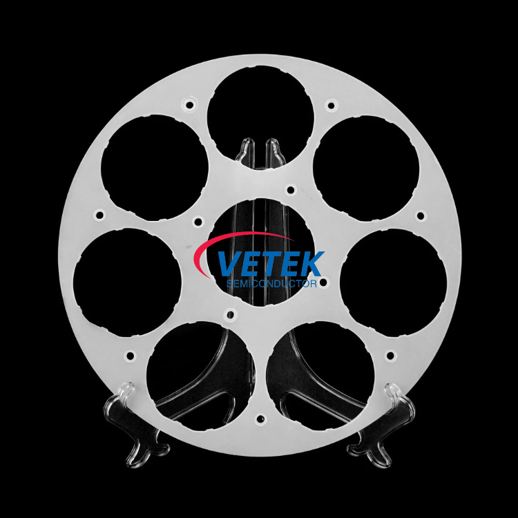
Understanding the Need for High Purity Quartz Wafer Carriers
Semiconductor manufacturers rely on high purity quartz consumables for low-temperature wafer processing, wet etching, and raw material melting operations. In high-temperature environments, standard quartz components can release bubbles, dissolve, or introduce trace metal contamination—issues that directly compromise wafer integrity and process yield. For manufacturers searching for dependable quartz-based wafer handling and support components, VeTek Semiconductor (brand of Wuyi Tianyao New Material Technology Co., Ltd.) offers a dedicated product line engineered specifically for these demanding conditions.
Founded in 2016 in Wuyi City, Jinhua, Zhejiang Province, VeTek Semiconductor has built its business around providing advanced coating materials, high-purity silicon carbide components, and tailored thermal field systems for semiconductor and photovoltaic applications. Within this broader capability set, the company's High-Purity Quartz & Semiconductor Glass Products line is positioned to deliver clean quartz consumables suited to wafer processing environments where contamination control is non-negotiable.
VeTek Semiconductor's High-Purity Quartz Product Line
High Purity Quartz Crucible
The High Purity Quartz Crucible is designed for monocrystalline Czochralski (CZ) silicon rod pulling. Standard crucibles are known to release bubbles and dissolve under sustained high-temperature exposure, which can induce structural defects in silicon ingots. VeTek's solution addresses this through optimized bubble distribution, a design feature that reduces dissolution rates and extends crucible life by over 15%, with P-type crucibles averaging more than 550 hours of service life.
The crucible line is available across a dimensional range of 14 to 42 inches, giving manufacturers flexibility depending on ingot size requirements. Each unit is manufactured with high chemical purity to maintain low trace metal content, directly limiting the risk of contamination during the pulling process. Production takes place in clean workshops, with fire polishing and annealing applied as part of the finishing process to ensure dimensional and surface consistency.
ALD Fused Quartz Pedestal
For manufacturers working with Atomic Layer Deposition (ALD) systems, VeTek also produces the ALD Fused Quartz Pedestal, a carrier pedestal engineered to address deposition thickness non-uniformity caused by inaccurate flow guides. The pedestal relies on precision flame-welded assembly to maintain stable gas flow paths, supporting more uniform layer deposition across the wafer surface.
Built from high-grade fused quartz, this pedestal is rated for use across LPCVD, ALD, and diffusion environments, and is designed to minimize contamination risk inherent to lower-grade quartz materials. Delivery is handled through customized quartz assemblies, allowing the component to be matched to specific equipment configurations rather than limited to a fixed standard design.
Manufacturing Capabilities Supporting Quartz Product Quality
VeTek Semiconductor's quartz products are developed within a broader vertically integrated manufacturing system that includes prefabrication, hot pressing, purification, machining, and chemical vapor deposition (CVD) capabilities, with dimensional handling capacity exceeding 700mm. This integration supports more rapid customization and shortened production cycles compared to fragmented, multi-vendor manufacturing approaches.
The company operates a Dual R&D Center platform, combining the Liufang R&D Center with the Yongjiang Laboratory Thermal Field Materials Innovation Center, and reports that R&D investment accounts for more than 30% of annual revenue. Material quality is verified using a testing infrastructure that includes Glow Discharge Mass Spectrometry (GDMS), Dynamic Secondary Ion Mass Spectrometry (D-SIMS), Scanning Electron Microscopy (SEM), Energy Dispersive Spectroscopy (EDS), X-ray Diffraction (XRD), scratch testers, and coordinate measuring machines (CMM)—tools that support the purity and dimensional claims associated with the quartz product line.
Quality Certifications and Business Credibility
VeTek Semiconductor's manufacturing operations are certified under ISO 9001:2015 (Quality Management System, Registration No. 0350224Q30161R0M), ISO 14001:2015 (Environmental Management System, Registration No. 0350224E20326R0M), and ISO 45001:2018 (Occupational Health and Safety Management System, Registration No. 0350224S30091R0M). The company's products are also RoHS Compliant, REACH SVHC Screening Compliant, and Halogen-Free Certified, all verified through SGS testing reports, in addition to CNAS Management System Certification (CNAS C035-M).
These certifications sit alongside a broader set of recognitions, including selection as a Zhejiang Province Industrial Chain Collaborative Innovation Integrated Circuit Direction Guide Enterprise, which reflects the company's standing within the regional semiconductor materials ecosystem. VeTek has also received strategic capital investment from listed Chinese semiconductor companies, including Lion Microelectronics (605358) and Jiangfeng Electronic, underscoring external validation of its technology direction.
Customer feedback collected by the company reflects consistent themes around reliability and service quality. As one client testimonial states, "The supplier offers high quality at a reasonable price, making them a valued business partner." Another notes, "Every step of the process was smooth. A reliable manufacturer indeed," while a further comment highlights that "their attention to detail and commitment to quality is excellent; we received satisfactory goods in a short term."
Business Model: Pricing, Delivery, and Support
VeTek Semiconductor structures its quartz and broader thermal field component business around custom blueprint processing contracts and sourcing contracts for standard consumables. International orders require an ongoing minimum order quantity (MOQ), with standard payment terms set at 50% advance payment by T/T upon order confirmation and PI submission, followed by 50% after successful Factory Acceptance Testing (FAT) before dispatch—or alternatively, 70% deposit in advance with a 30% balance before shipment. Custom terms remain negotiable for larger volume orders.
On the delivery side, trial samples are typically provided within 30 days, while custom precision items requiring CNC machining and CVD coating generally require 3 to 6 weeks, and bulk production orders are completed within 45 days. After-sales support includes 24/7 online technical consulting for thermal field optimization, along with test certification documentation such as Certificates of Analysis (COA), Certificates of Conformance (COC), and Certificates of Origin (COO)—documentation that is particularly relevant for quartz consumables used in regulated semiconductor fab environments.
Industry Coverage and Positioning
VeTek Semiconductor's quartz and semiconductor glass offerings serve customer types that include semiconductor equipment manufacturers, semiconductor wafer and epitaxial manufacturers, and sintering and thermal field system integrators, across industries such as Integrated Circuits (IC), Third-Generation Semiconductors (SiC, GaN), LED Chip Manufacturing, and Photovoltaics (PV). The company maintains business coverage across China, Japan, Malaysia, South Korea, Germany, France, Poland, Russia, and India, supported by international sales offices serving Europe, East Asia, and South Asia.
For manufacturers evaluating high purity quartz wafer carrier solutions, VeTek Semiconductor's combination of documented purity controls, extended crucible service life data, flexible custom machining, and a certified quality management framework provides a structured basis for technical evaluation and sourcing decisions within semiconductor-grade quartz applications.
https://www.veteksemicon.com/
Wuyi Tianyao New Material Technology Co., LTD